Oculus Quest 2 is Facebook’s follow-up to the original 2019 Quest, offering a higher resolution display, higher refresh rate, lower overall weight, and a more powerful Qualcomm Snapdragon XR2 chipset. A teardown of Quest 2 shows most of the headset’s innards, splayed out for all to see.
Not a few hours after receiving Quest 2, Japanese Twitter user ‘GOROman’ has done a near-complete teardown of the device, showing off some interesting design choices that seem to differ from last year’s model.
The short of it: Quest 1 is starting to look (dare I say) a little primitive, what with its soldered wires, single copper heat pipe and off-the-shelf fan unit. Quest 2’s teardown reveals plenty of LEGO-snappy ribbon cables and an even more densely packed interior. Check out the teardown of Quest 1 here.
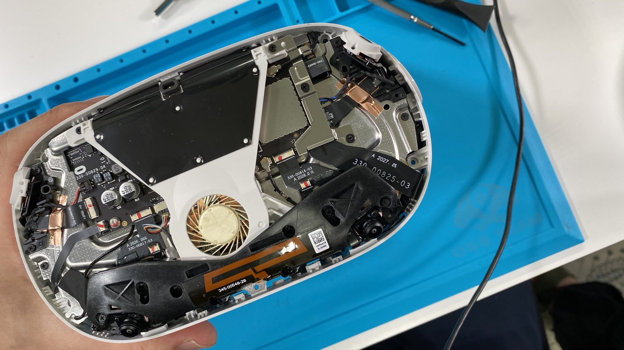
Here’s one of the first images, which shows the headset’s front shroud removed and exposing the internal fan covering. It’s already easy to tell that Oculus has shrunk just about everything to shave off the weight, taking the Quest hardware platform from 571 g (20.1 oz) down to 503 g (17.7 oz).


Removing that fan covering and black plastic bracing below it reveals a fan-shaped heatsink extending upward.


Here’s a beauty shot of the left side of the motherboard before GOROman removes it. That looks like an insane amount of work to teardown. It’s a shame iFixit hasn’t taken the opportunity yet to give us a detailed play-by-play in English so we can hear a summary of the process and a rating for fixability.
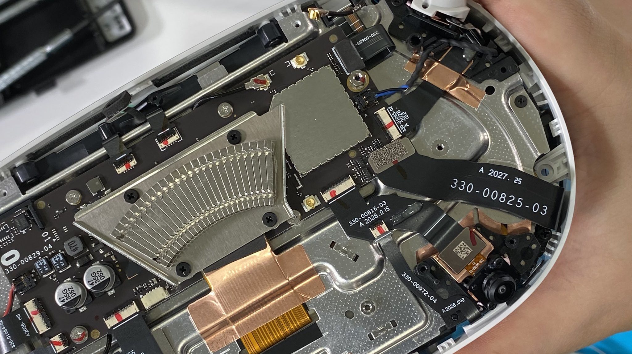
Heatsink removed, we can now see the Snapdragon XR2 chip, replete with thermal compound for ensuring good heat transfer from the chip to the heatsink. On the left you can just make out the headset’s internal storage, built by SanDisk.
Everything here is so close together, which is probably to make better use of the fan + heatsink combo; last year’s model had a more distributed cooling solution that didn’t directly connect to a heatsink.
Removing the motherboard entirely and we find more thermal compound on what appears to be an EM shield doubling as a passive cooling heatsink.
Then he removes the EM shield entirely, which reveals that it’s really two sandwiched units that provide a platform for the headset’s external sensors. Those are used for positional tracking, passthrough, and hand tracking.
Flipping it over you can see that the supposed EM shield is sandwiched onto the back of the display assembly, which includes the IPD switch mechanism and single near 4K LCD display, which means effectively 1,832 × 1,920 resolution served up per-eye. Remember kids: no liquid cleaners!
With the main bits done (and probably a million screws removed), lets take a look at the battery. That’s a 3,640 mAh (14.0 Wh) lithium-ion pack – same capacity as last year.
Interestingly enough, it’s actually one of the first pieces you’ll see when disassembling the headset, as it sandwiches between the Quest 2’s guts and the top interior of the white plastic casing. Here’s GOROman screwing back into place during reassembly. Yes, he really put it all back together.
It’s nice to know you don’t need to destroy anything to get inside, and provided you had a replacement part and knew what to remove, you might actually be able to swap parts without de-soldering things. That’s coming from someone who has little hands-on experience with willfully voiding manufacturer warranties though. And if I have to say: this will void your warranty.
One of the things GOROman didn’t manage was a teardown of the new Touch controllers, although we’re betting not much has changed. Also, a look inside the lens assembly would have been a treat to see just how the IPD adjuster works. Then again, it’s only been a few hours since Quest 2 landed on consumer doorsteps, so there’s plenty of time for the Internet boffins to poke around.
You can check out GOROman’s full teardown and reassembly below. It’s in Japanese, and over 2 hours long, although it’s still worth scrubbing through to give you an idea just how fiddly and tightly packed the headset’s internals are.
